James Bryant Consultant Engineer - Analog Electronics
RTFDS
How to make Sense of a Data Sheet
This is the first of a series of short articles on problems in analog electronics which can be addressed by an enlightened study of the data sheet concerned. Links to the other three are at the bottom of the page.
My duties as an Applications Engineer include answering the telephone to customers and potential customers who have questions about Analog Devices’ products. I hope that I am usually polite and helpful, and I do endeavour to anticipate questions which might arise from further study of the device concerned after my caller has hung up, and to answer them before they are asked. However, like all Applications Engineers, I have moments when my patience is strained. When this happens the commonest reason is the one which causes me, as I hang up, to shout “RTFDS”. The shout is invariably echoed by every other Applications Engineer within earshot.
RTFDS stands for “Read The Friendly Data Sheet” and I am driven to utter it when my customer, during his phone call, clearly demonstrates that he has not even looked at the data sheet of the device that he is enquiring about before calling me. F****** might stand for many other things. It might be factual, familiar, fascinating, final, fine, fitting, fluent, formal, frank, friendly, or full; but we shall hope that it is not facetious, facile, faithless, fantastic, farcical, faulty, featureless, feeble, felonious, fictitious, filthy, flippant, foolish, foul, fretful, Freudian, frustrating, fulsome, fusty, or futile. Other, less likely, possibilities might include fabulous, faint, fair, faithful, fallen, fallible, false, famous, fanciful, fancy, farinaceous, fascist, fashionable, fat, fateful, fatherly, fatiguing, favourite, fearful, fearless, fecund, feline, feminist, fertile, fervid, festive, fetching, feudal, fibrous, fickle, fiddly, fiery, filigreed, finished, finite, firm, fitful, fixed, flabby, flaky, flamboyant, flaming, flashy, flat, flea-bitten, fleshy, flighty, flossy, flowery, fluid, flying, foggy, folded, footloose, forbidden, foremost, forged, forlorn, former, forthcoming, fortuitous, fortunate, fossilised, fractious, framed, frantic, fraternal, fraught, freak, free, frenetic, frenzied, fresh, frightful, frigid, frisky, frivolous, frizzy, frolicsome, frosty, frugal, fruity, frumpish, frustrated, fuddled, fugitive, fulminating, fuming, functional, fundamental, funereal, fungoid, funny, furry, furled, furtive, fussy, fuzzy or whatever. While we all hope that you feel warm and fuzzy after you’ve read a data sheet it would be inappropriate for the data sheet itself to be that way.
If this article ensures that no customer ever again calls to ask a question that is answered conspicuously on the front page of the data sheet I shall probably be canonised by my grateful fellow Applications Engineers as St. James Bryant. (I really did once have someone call to ask how many pins there are on an 8 lead minidip. I was polite to him!) Nevertheless there is another issue which should also be considered under the same title - how to interpret a data sheet. If we understand the conventions and constraints involved in the production of an IC data sheet we are far better able to extract the information which is present by implication but is not explicitly written into it.
The ostensible purpose of a data sheet is to provide the user and potential user with the fullest possible information about the functions and technical characteristics of the device concerned. But there are other agendas as well. The IC Designer who writes the first draft of the data sheet wants to demonstrate to the World what a wonderful designer he is and what a superlative product he has designed. This results in an emphasis on its good parameters and neglect of all others. The Product Marketing Engineer who edits the Designer’s work will also want to avoid any downside to the device performance, but he will also try to stress any competitive advantages over other manufacturers’ products and to emphasise features, like motherhood and apple pie in another context, which are universally believed to be beneficial. (Consider two devices from the Analog Devices Catalog:- one, the AD8500, has a dissipation, in normal operation, of 1.5µW, the other, the AD9690, has a dissipation of 1.5 W, one million times greater. Both are described on the front pages of their respective data sheets as “low power”. I really do believe that one day I shall live to see an IC advertised as “cholesterol free”.)
The next contributor is the Test Engineer, who, in the interests of minimising the time and cost of production testing, tries to remove all maxima and minima from the table of characteristics and replace them with “typical” values (ideally the Test Engineer would like the specification to be such that if the device has the correct number of leads, give or take one or two, it will pass its final test). He is followed by a Lawyer (Henry VI, Act IV, Scene 2, Line 82) who wants to insert a few dozen pages of fine print emphasising that whatever happens when the device is actually used it wasn’t our fault, we told you not to, and we are not liable (and if you infringe our patents we’ll want some money). After the Lawyer has finished someone from Corporate Communications wants to ensure that the Data Sheet is shrunk from sixty pages to four and is in the Company Standard Format, and that it bears a date and publication number and the address of every company office and agent from Aarhus to Zyryanovsk.
It is now the turn of the Applications Engineer. His motives are just as base as all the others, but his ideal is to be able to spend his afternoons asleep in the office without being disturbed by customers on the telephone. To achieve this he must make the data sheet so clear and simple that even Dan Quayle or a software engineer can understand it.
This is not as simple as it may appear since he will be in conflict with the other contributors. There is generally little difficulty in including specifications of the basic parameters of the device (Vos, Ib, Aol, GBW, slew rate and a few more in the case of an op amp, for instance). What is more difficult is to include specifications which the Designer and Product Marketing Engineer are less proud of: for instance, that the device latches up and destroys itself if the negative supply is applied before the positive supply. The Applications Engineer (and the Lawyer) regard it as very important that such data is available, but they probably will not be allowed to have a little red box on page 1 saying “If you apply Vss before Vdd you’ll blow the bugger up”.
Subtlety allows us to pass the information. If the “Absolute Maximum Ratings” section of the data sheet contains an entry of the type
Vss ≥ -Vdd or, better, |Vss| ≤Vdd
this tells us that the absolute amplitude of the negative supply must never exceed the amplitude of the positive supply. The problem, from the Applications Engineer’s viewpoint, is that many people who read the data sheet assume that ICs can foresee the future and that these ratings allow you to apply a negative supply before the positive supply, on the grounds that when the positive supply arrives it will be larger than the negative one and all will be well. This is not the case - if a parameter, B, in the Absolute Maximum Ratings of a device is expressed in terms of another parameter, A, this is a clear instruction that whatever the instantaneous values of A, the value of B must remain within the limits so defined at all times.
Such definitions in the Absolute Maximum Ratings allow us to convey information about potential power up sequencing and signal/power sequencing problems without the stigma (as perceived by marketing types) of a clear explicit warning.
There are other parameters which are implicit in the data sheet rather than formally stated. An example is current noise, which is relatively rarely specified. It is unnecessary to specify current noise in many cases because devices whose input is a simple bipolar transistor or FET have input current noise which is the Schottky noise of the input bias current. (This is not true, however, for devices, such as current feedback amplifiers, rail to rail input amplifiers, or bias compensated amplifiers like the OP 07 or OP 177, where the device input connects to a node within relatively complex circuitry rather than to the otherwise unconnected base or gate of a single device.) For such a simple device the noise current density is √2qIb Amps/√Hz where Ib is the device bias current (in amps) and q is the charge on an electron (1.6 x 10⁻¹⁹ Coulombs).
Even where we do not know that a device has a simple input structure this calculation allows us to set a minimum value for current noise, since it cannot be less than the Schottky noise of the bias current.
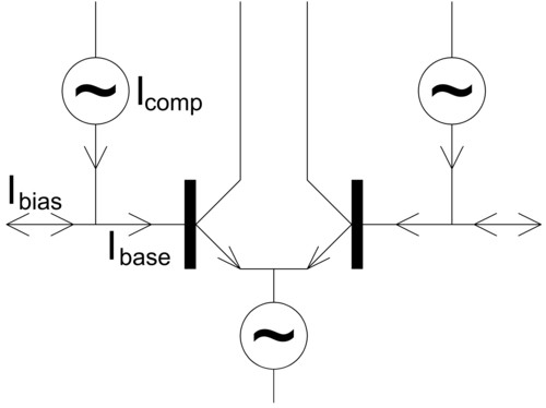
You might suppose that we can determine the input structure of a device by consulting the circuit diagram on the data sheet. Unfortunately both the Designer and the Lawyer simplify this important figure in order to conceal proprietary structures from our competitors. The diagram you see on the data sheet does bear some resemblance to the circuitry on the chip, but not very much. It is sometimes possible to infer more about the structure from studying other parameters. For example, “bias compensated” amplifiers like the classic OP-07 have input stages where the bias current of the input transistors is provided by current sources on the chip as shown below.
It is evident that in the ideal case where Icomp = Ibase the bias current, Ibias, will be zero. In real life they will not be equal and the direction of the bias current will depend on which is the larger. The data sheet should show Ib with a bipolar value (±X nA). If we find a data sheet where a bias current does not show the possibility of bipolar flow and the circuit diagram shows bias compensation or, conversely, we find one where the diagram shows a simple input stage with a single long tailed pair but the bias current is defined as bipolar then we may infer that something is incorrect, or at the very least incomplete. (Note that rail rail input stages also have bipolar bias currents, but in this case the bias current varies with common mode voltage and will always flow one way when the input is near the positive rail and the other when it is near the negative, with bias compensated inputs the direction of flow is unpredictable.)
The Test Engineer is not always successful in eliminating maxima and minima from the specification. If a maximum or minimum value of a parameter is specified, then, under the range of operating conditions for which it is specified, the parameter is guaranteed not to be greater than the maximum or less than the minimum values. This is generally guaranteed by testing the parameter but in some cases may by be “guaranteed by design”. This means that the design of the device ensures that if certain parameters which are tested remain within their correct ranges then others will also do so and need not actually be tested. At Analog Devices we distinguish the two on our data sheets by printing parameters which are tested for minima/maxima in bold type. However, the fact that a parameter is not tested should not imply that maximum/minimum information is any less reliable.
The meaning of “maximum” and “minimum” is clear and well understood. The meaning of “typical” is open to many interpretations. The simplest is the “mean” or “average” value over a large number of devices and for some parameters, such as current consumption, this is not unreasonable. But the average value of offset voltage for a large number of op amps should be zero, if it is not zero the design has some systematic bias which should have been corrected. So in such a case the “typical” value cannot be a simple mean but will probably be the mean of the modulus of the value.
The distribution of values about the “typical” value when the device is first tested is frequently Gaussian, but it may not be when the device is shipped. Consider as an example a device which is available in three grades, selected by a single parameter: “A” grade ±1%, “B” grade ±2%, and “C” grade ±5%. During the final test it is obvious that any device whose output is within ±0.9% (to leave a small test margin) will be binned as “Grade A”, etc. However, if the device has been well designed and manufactured it may well be that 90% of production meets the “A” specification, while 90% of the orders are for the “C” grade, accordingly many devices from the “A” bin will be branded and sold as “C” grade. In this case the distribution of devices that are shipped as “C” will be very near Gaussian with a narrow distribution and most will, in fact, meet the “A” specification. If, on the other hand, there is a high demand for “A” and “B” grade devices and the specification is hard to meet then devices shipped as “C” grade will contain no devices which meet the “A” or “B” specifications and the distribution of parameters will be far from Gaussian.
(An interesting side effect of the first case above occurs where the demand for “B” grade devices is low. In such a case all “B” devices may be supplied from the “B” bin, while most “C” devices are supplied from the “A” bin. Since the “B” bin contains no “A” devices this will mean that the average quality of “B” devices is far worse than the average quality of “C” devices! Responsible manufacturers avoid this by eliminating the “B” bin in such a case, supplying all “B” devices from the “A” bin, and saving a little on test and handling costs.)
Tables of minimum, maximum and typical values do not tell us much about the behaviour of a device under non standard operating conditions. (Neither do the majority of “Spice” macro models, which are generally simplified for fast execution and are not intended for detailed analyses of non standard operation. The more complex “Spice” models used by the circuit’s designers are rarely published because they would provide competitors with too many insights.) Today, when many designers require circuits to operate with ±5 V or even +5 V or +3 V supplies, rather than the traditional ±15 V, it is quite common to provide separate tables of parameters for ±15 V, ±5 V, +5 V and +3 V operation. It is also common for engineers to call the Applications Department to request details of behaviour at intermediate (and sometimes indeterminate!) values of supply.
It is rare for Applications Engineers (or, indeed the original designer) to have detailed information about such behaviour but it is usually possible to infer how the device will behave from the information that is published. (If the behaviour of a particular parameter is critical to a large volume application we are sometimes prepared to perform a special test to ensure that devices so tested are suitable for the application but special testing is expensive, and should be avoided wherever possible.)
If the values of a parameter vary little between the stated values of supply it is most unlikely that they will vary much at intermediate values either. However it is not safe to assume that they will continue to be well behaved outside this range. Some data sheets specify a range of supply voltages over which the device will perform to specification and some have graphs showing (typical) variations of behaviour plotted against variations of variables which may include supply, temperature, common mode voltage, output current, etc. Using this information it is often possible to predict how a device will behave under non standard conditions, but it is always necessary to check the prediction by experiment.
The problem with such experiments is determining how representative they are of the behaviour of other devices of the same type. If the available data, and the nature of the circuit, suggest that a parameter will vary gracefully as some variable is changed, and experiment with a few devices from different batches confirm that it does indeed do so then it is reasonable to assume that the majority of devices will behave in the same way. On the other hand, if graphs in the data sheet (or our own measurements) show discontinuities then it may be less safe to make reasonable interpolations.
So far we have considered cases where we can infer more from a data sheet than is explicitly written there. There are cases, though, where engineers make assumptions which are not justified by the data which is actually given on the data sheet. This is particularly common with digital signals.
Consider an Analog Digital Converter (ADC) which has an END OF CONVERSION (EOC) output. When we command a conversion EOC goes high and when the conversion is complete it goes low again. Many engineers attempt to use the falling edge of EOC to read the data from the ADC. Some, with some ADCs, succeed, but many discover that EOC signals that conversion is complete but NOT that data is available, which is not the case for another few nSec. The data sheet almost always provides this information but, as I have said, too many engineers do not RTFDS but assume that if the conversion is complete the data is available. (It would be better if all ADC designers provided DRDY, which is not asserted until the data is valid and ready to read. Many do, but new ADCs are still being designed which assert EOC a few nSec before the data becomes valid.)
Similarly CE (chip enable) is assumed to power up a device from standby. It may also act as a reset, a clock synchroniser, or other functions. A CE which only enables a chip may be hard wired low. If it performs other operations the chip will not operate with CE tied low. The data sheet will tell you if you bother to read it..
This article was prompted by reflections on a career spent in Integrated Circuit Applications. The single largest cause of user problems in my field is lack of attention to signal routing, grounding and decoupling, but the next is undoubtedly failure to read and understand the data sheet. Among the common notices which people hang over their desks (“You Don’t Have To Be Crazy To Work Here But It Helps”, “This Is A Non Profit Organisation But We Didn’t Mean It To Be That Way”, etc.) is one which says “When All Else Fails Read The Instructions”. I should like to change that one to “Before It Fails RTFDS”. We have seen that there is considerably more information available in a data sheet than is given explicitly. It is well worthwhile learning to consider the implications of a data sheet when studying the parameters and specifications on it, as it is usually possible to deduce a considerable amount of valuable information. In most cases actually reading the friendly data sheet, followed by a little intelligent deduction can make calling the Applications Department unnecessary and I can sleep on undisturbed.
Newbury - England 1995-08-05
Revised 2015-10-10
[Note that although this has been revised, many of the examples still date back 20 years to the original article.]