James Bryant Consultant Engineer - Analog Electronics
RTFDS-3
The DC Specifications of ADCs & DACs
This one of a series of short articles on problems in analog electronics which can be better understood by an enlightened study of the data sheets and is intended as an introduction to the meaning of the DC parameters specified on the data sheets of digital to analog and analog to digital converters (DACs and ADCs respectively). Long experience as an Applications Engineer has convinced me that the exact meaning of ADC and DAC specifications is frequently misunderstood. A future article will discuss AC specifications.
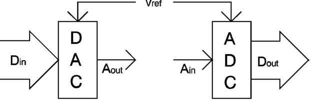
DACs and ADCs are interfaces between the analog and digital worlds. A DAC is a device which gives an analog output related to a digital input, while an ADC gives a digital output in response to an analog input. While DACs and ADCs can be made with deliberately non-linear transfer characteristics, they are not considered here. With the exception of these rare cases a DAC is a circuit whose analog output is proportional to its analog reference and to the value of its digital input. Conversely an ADC is a circuit whose digital output is proportional to the ratio of its analog input to its analog reference. (Often, but by no means always, the scaling factor between the analog reference and the analog signal is unity, so the digital signal represents the normalised ratio of the two.)
Fig 1. Digital-Analog (DAC) & Analog-Digital (ADC) Converters.
(The analog signals are generally voltage, current or, sometimes, resistance.)
The most important thing to remember about both DACs and ADCs is that one of the signals is digital, and therefore quantised. This is to say that an N-bit word represents one of 2N possible states and therefore an N-bit DAC (with a fixed reference) can have only 2N possible analog outputs, and an N-bit ADC can have only 2N digital ones.
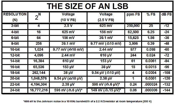
The parameters of data converters may be expressed in several different ways: lsbs, parts per million of full scale (ppm FS), millivolts (mV), etc. Different devices (even from the same manufacturer) will be specified differently, so converter users must learn to translate between the different types of specification if they are to compare devices successfully.
Fig 2. The size of an LSB.
(A simple technique to memorise this table is to remember that at
10-bits and 10 V FS an lsb is approximately 10 mV, 1,000 ppm or 0.1%. All other values may be calculated by powers of 2.)
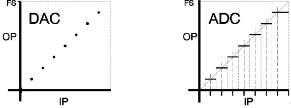
Fig. 3 shows the ideal transfer characteristics for a 3-bit unipolar DAC and a 3-bit unipolar ADC. In the former case both the input and the output are quantised and the graph consists of eight points - while it is reasonable to discuss the line through these points it is very important to remember that the actual transfer characteristic is not a line but a number of discrete points.
Fig 3. Ideal Converter Transfer Characteristics.
The input to an ADC is analog and is not quantised, but its output is quantised, the transfer characteristic therefore consists of eight horizontal steps (when considering the offset, gain and linearity of an ADC we consider the line joining the midpoints of these steps).
In both cases digital full scale (all 1s) corresponds to 1 lsb below the analog full scale (the reference or some multiple thereof). This is because, as mentioned above, the digital code represents the normalised ratio of the analog signal to the reference and if this were unity the digital code would be all 0s and 1 would be in the bit above the msb.
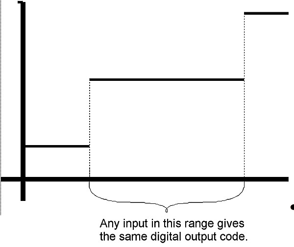
Fig 4. Quantisation Error.
(Analog input of ±½ lsb on nominal gives the same digital output.
This is the “quantisation uncertainty” or “quantisation error”.)
As shown in Fig 4 the (ideal) ADC transitions take place at ½ lsb above zero and thereafter every lsb until 1½ lsb below analog full scale. Since the analog input to an ADC can take any value but the digital output is quantised there may be a difference of up to ½ lsb between the actual analog input and the exact value of the digital output. This is known as the "quantisation error" or "quantisation uncertainty". In AC (sampling) applications this quantisation error gives rise to "quantisation noise" which we shall not discuss in this article.
There are many possible digital coding schemes for data converters: binary, offset binary, 1's compliment, 2's compliment, gray code, BCD and others. This article, being devoted to the analog specifications of data converters, will use simple binary and offset binary in its examples and will not consider any others.
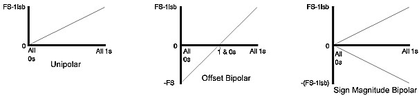
Fig 5. Unipolar & Bipolar Converters.
(Other digital codes are possible - these are the commonest.)
The examples in Fig. 3 use unipolar converters, whose analog port has only a single polarity. These are the simplest type, but bipolar converters are more generally useful. There are two types of bipolar converter: the simpler is merely a unipolar converter with an accurate 1 msb of negative offset (and many converters are arranged so that this offset may be switched in and out so that they can be used as either unipolar or bipolar converters at will), but the other, known as a "sign magnitude" converter is more complex and has N bits of magnitude information and an additional bit which corresponds to the sign of the analog signal. The transfer characteristics of these different types are shown in Fig 5. Sign magnitude DACs are quite rare, and sign magnitude ADCs are found mostly in digital voltmeters (DVMs).
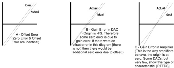
Fig 6. Offset and Gain Error in Converters.
(Most bipolar converters' transfer characteristics have their origin at -FS, so their zero error contains both offset and gain error contributions, unlike amplifiers, whose offset and zero error are generally identical and unaffected by gain error.)
I do not wish to discuss such specifications as absolute maximum supply or signal voltage, current consumption, and power dissipation as these are common to most, if not all, ICs. I shall consider the four DC errors in a data converter which are relevant to its performance as a converter:- offset error, gain error and two types of linearity error. Offset and gain error are analogous to offset and gain error in amplifiers. (Though offset error and zero error, which are identical in amplifiers and unipolar data converters, are not necessarily identical in bipolar converters and should be carefully distinguished - see Fig 6.) The transfer characteristics of both DACs and ADCs may be expressed as:-
D = K + GA
Where D is the digital code, A is the analog signal, and K and G are constants. In a unipolar converter K is zero and in an offset bipolar one it is -1 msb. The offset error is the amount by which the actual value of K differs from its ideal value. The gain error is the amount by which G differs from its ideal value (and is generally expressed as the percentage difference between the two, although it may be defined as the gain error contribution [in mV or lsb] to the total error at full scale). These errors may generally be trimmed by the data converter user. (Note, however, that although in an amplifier offset is trimmed at zero input and then the gain is trimmed near to full scale, the trim algorithm for a bipolar data converter may not be so straightforward - most bipolar converters are trimmed for offset near -FS and for gain near +FS, but some, like amplifiers, are trimmed at zero and near FS. RTFDS!)
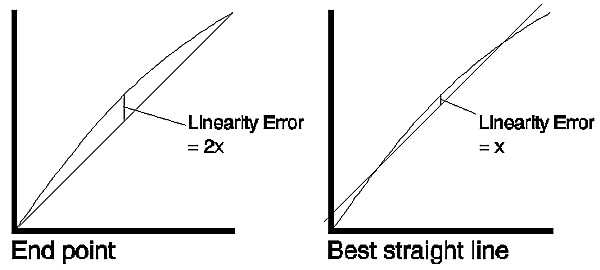
Fig 7. Methods of Measuring Converters' Integral Linearity.
(The same converter is shown on both plots.)
The integral linearity error of a converter is also analogous to the linearity error of an amplifier and is defined as the maximum deviation of the actual transfer characteristic of the converter from a straight line. It is generally expressed as a percentage of full scale (but may be given in lsbs). There are two common ways of choosing the straight line:- end point and best straight line. These are shown in Fig 7.
In the end point system the deviation is measured from the straight line through the origin and the full scale point (after gain adjustment). This is the most useful integral linearity measurement for measurement and control applications of data converters (since error budgets depend on deviation from the ideal transfer characteristic, not from some arbitrary "best fit") and is the one normally adopted by Analog Devices Inc.
The best straight line, however, does give a lower value of "linearity error" on a data sheet. Here the best fit straight line is drawn through the transfer characteristic of the device using standard curve fitting techniques, and the maximum deviation is measured from this line. In general the integral linearity error measured in this way is only 50% of the value measured by end point methods - which makes the method good for producing impressive data sheets, but it is less useful for error budget analysis. (For AC applications best straight line linearity is a better measure of distortion than end point linearity but it is even better to specify distortion directly.) Analog Devices uses best straight line linearity on data sheets only in the case of second-source products where the original manufacturer's data sheet used best straight line, rather than end point, linearity. Otherwise we always specify end point linearity.
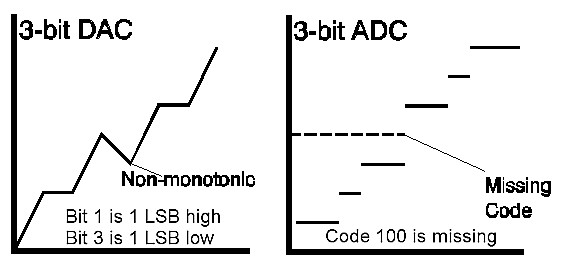
The other type of converter non-linearity is "differential non-linearity" (DNL) which is illustrated in Fig 8. This relates to the linearity of the code transitions of the converter. In the ideal case a change of 1 lsb in digital code corresponds to a change of exactly 1 lsb of analog signal (in a DAC a change of 1 lsb in digital code produces exactly 1 lsb change of analog output, while in an ADC there should be exactly 1 lsb change of analog input to move from one digital transition to the next).
Fig 8. Differential Non-Linearity.
Where the change in analog signal corresponding to 1 lsb digital change is more or less than 1 lsb there is said to be a DNL error. The DNL error of a converter is normally defined as the maximum value of DNL to be found at any transition.
If the DNL of a DAC is <-1 at any transition the DAC is "non-monotonic" (i.e. its transfer characteristic contains one or more maxima or minima). A DNL >+1 does not cause non-monotonicity, but is still undesirable. In many DAC applications (especially closed-loop systems where non-monotonicity can change negative feedback to positive feedback) it is critically important that DACs are monotonic and monotonicity is often explicitly specified on data sheets, although if the DNL is guaranteed to be less than 1 lsb (i.e. lsb) then the device must be monotonic, even without an explicit guarantee.
ADCs can be non-monotonic, but a commoner result of excess DNL in ADCs is missing codes. Missing codes (or non-monotonicity) in an ADC are as objectionable as non-monotonicity in a DAC and as much to be avoided. Again, they result from DNL<-1 lsb.
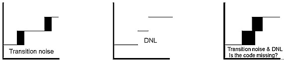
Fig 9. Combined effects of transition noise & DNL.
(The same converter is shown on both plots.)
Defining missing codes is more difficult than defining non-monotonicity. All ADCs suffer from some transition noise (think of the flicker between adjacent values of the last digit of a DVM). As resolutions become higher the range of input over which transition noise occurs may approach, or even exceed, 1 lsb. In such a case, especially if combined with a negative DNL error, it may be that there are some (or even all) codes where transition noise is present for the whole range of inputs. There are therefore some codes for which there is no input which will guarantee that code as an output, although there may be a range of inputs which will sometimes produce that code.
For lower resolution ADCs it may be reasonable to define "no missing codes" as a combination of transition noise and DNL which guarantees some level (perhaps 0.2 lsb) of noise-free code for all codes, but this is impossible to achieve at the very high resolutions, as high as 24-bits, achieved by modern Σ-Δ converters, even though these converters can be demonstrated, both theoretically and by testing, to be free of missing codes. In these cases the manufacturer must define noise levels and resolution in some other way. It is common to provide a table of effective resolution v filter bandwidth.
Newbury - England 1995-08-05
Revised 2015-10-10
[Note that although this has been revised, many of the examples still date back 20 years to the original article.]