James Bryant Consultant Engineer - Analog Electronics
RTFDS-1
Operational Amplifier Bias Currents
This one of a series of short articles on problems in analog electronics which can be better understood by an enlightened study of the data sheet concerned.
The ideal op amp beloved of text book writers has specifications which are all either zero or infinity, zero offset, infinite gain, zero noise, infinite bandwidth, etc. Unfortunately, as is also the case with those other ideals beloved of pedagogues, the perfect black body, the reversible heat engine, or, the favourite of lawyers and economists, the rational man, the ideal op amp has one other specification which is zero:- the number of examples of the ideal which have ever existed or will ever exist. We live in an imperfect World.
This article considers one parameter of a real op amp, its bias current. It is a very widely varying parameter: some electrometer op amps have Ib of a few fA while the fastest wideband ones may have Ib as large as 10 µA - a range of one billion to one. It is enlightening to consider a number of different op-amp input stages and their differing bias current characteristics.
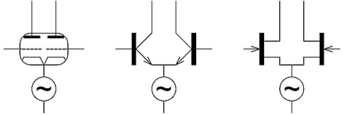
Basic op-amp input stages are illustrated in Fig. 1.
Fig 1. Basic op-amp input stages.
This structure, which has differential voltage input and differential current output and is fairly insensitive to common mode input variations, is known as the “long tailed pair” and it may be built with thermionic valves (which were used for the very first op amps but are now effectively obsolete in this application) or with bipolar or field effect transistors. All classical or “voltage feedback” op amps use some variation of this structure but within the last decade a different type of op amp, known as the “transimpedance” or “current feedback” op amp, has become popular for HF applications and we shall consider that structure later in the article.
Let us consider the bipolar transistor structure first. Although it is most practical to analyse it as a voltage, or, more strictly, a transconductance, amplifier stage when considering its behaviour as an amplifier, it is easiest to analyse its bias current by considering the bipolar transistor as a current amplifier. The transistors have a current gain of β, so the collector current, Ic, is β times the base (or bias) current, Ib. In the balanced condition half the tail current will flow in each transistor, so if the tail current is Itail then Ib will be approximately Itail/2β (this approximation assumes β>>1 and therefore Ic ≈ Ie).
Practical values of β for normal bipolar transistors are of the order of 100 (note that this is not of the close order of 100 - values will be between 30 and 500) and it is reasonable to assume that the β of the two well matched transistors of an op amp input stage will be matched to 1% or better and therefore the bias currents of a simple bipolar input op amp will be well matched. Moreover these currents do not vary much over the full operating temperature range of the op amp, perhaps 2:1 or 3:1 in the worst case, and remain well matched as they vary.
But they will not be very low. Even if the tail current is limited to 2µA (which will severely limit the practicable bandwidth of the stage) the bias current will be of the order of 10nA, and more practical tail currents of several tens of µA will result in bias currents of the order of hundreds of nA. High speed op amps of this type, where the tail current of the input stage may need to be around 1mA, may have bias currents as high as 10µA.
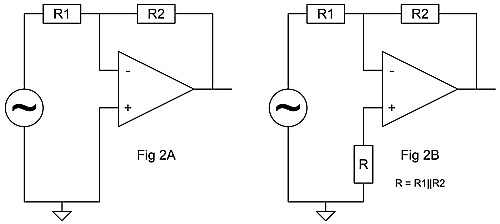
These currents will flow in the resistances present in the external op amp input circuitry and degrade the offset voltage, Vos, as shown in Fig. 2A.
Fig 2. Bias Current Compensation using an additional Resistor.
As Fig. 2B shows, we can compensate for this problem by the use of a “bias compensation resistor”, R, in the non inverting input which is equal in value to the resistance in the inverting input. In this case the bias current, Ib+, in the inverting input flows in the “bias compensation” resistor, R, (equal to the parallel combination of R1 & R2) and compensates for the offset error. But this technique works only when the bias currents in the inverting and non inverting inputs are closely matched - with many op amp input structures this is not the case.
Not all bipolar transistors have values of β of the order of 100. There is a special type of transistor with a very narrow base which has a β up to 50-100 times greater. This is known as a “super-beta” transistor. The price that is paid for this high β is a low breakdown voltage (due to the thin base) and high capacitance, and therefore somewhat limited frequency response.
Bipolar op amps with super-beta input stages can have Ib as low as a few tens of picoamps and their bias currents are fairly well matched, though not as well as those of normal bipolar types. Again, their bias current does not vary very much with temperature (a little more than normal bipolar op amps, perhaps 5:1 worst case). However, the technique is unsuitable for use in high speed op amps. The additional circuit complexity necessary to protect the super-beta devices from high supply voltages also makes their use impracticable in rail-rail op-amps. We shall discuss this last point later.
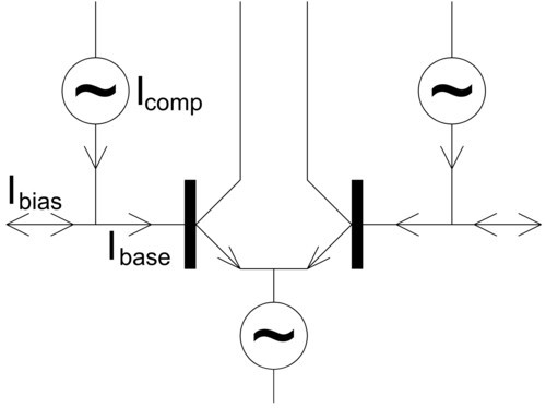
Not all IC processes are capable of fabricating super-beta transistors. There is another technique which may be used to reduce the bias current of a bipolar op amp input stage. This is also called “bias compensation” but has no connection with the technique involving a resistor which we discussed in Fig. 2. A bias compensated op amp is illustrated in Fig. 3.
Fig 3. On-chip Bias Current Compensation using Current Sources.
It consists of a standard bipolar long tailed pair with the addition of two current sources. These provide the base currents of the input transistors. If each current source provided exactly the base current required we would have the ideal situation that I mentioned above - zero Ib. In fact Icomp and Ibase are not exactly equal and so there is a residual external bias current Ib = Ibase - Icomp. For a given tail current, however, Ib is much lower and this technique is widely used in high precision op amps. The classic OP 07 and many other op-amps use this technique.
Like super beta, however, this technique does not lend itself to the design of high speed op amps, and it has another feature which can occasionally be inconvenient: the amplitude and direction of the small bias current depends on the mismatch between much larger currents. This means that Ib in such amplifiers can vary quite widely, and can indeed flow in either direction. The matching of Ib+ and Ib- is not particularly good (although they will be of the same order of magnitude) and they may even flow in opposite directions. The use of an external bias compensation resistor is therefore counterproductive with such devices.
Since the bias current of these bias compensated op amps may flow in either direction the data sheet will show a bipolar value (±XnA) for Ib. A bipolar Ib specification indicates that an op amp has a complex input structure and if a low frequency device has bipolar Ib and does not have rail-rail input common mode range it will almost certainly have bias compensation of the type we have just discussed.
So far we have discussed op amps with bipolar transistors in their input long tailed pair. If we replace these input devices with field effect transistors, either JFET or MOSFET, the bias current can be made much smaller. Nearly all BIFET (JFET) op amps use P channel FETs, although there are a few high speed devices which use N channel ones.
Bipolar transistors draw a base current which is proportional to their collector current. In theory FETs do not need to draw any gate current to operate. In practice there are leakage currents, which are the reverse leakage of a (silicon) diode. (In theory a MOSFET amplifier could be made which does not have diode leakage at its input - in practice this means omitting all protective circuitry and the gate oxide becomes so vulnerable to ESD as to be virtually unusable. Such devices have been made for specialised electrometer applications but are so rare as not to be worth considering in an article like the present one.) I shall treat both JFETs and MOSFETs under the single heading of FETs since their behaviour with respect to bias current (not necessarily in other respects) is virtually identical. The bias current of an op amp with a JFET input stage is, as I have said, the reverse leakage of the (silicon) gate diode (it could be germanium or GaAs but today virtually all op amps are made with silicon), and the bias current of an MOS device is effectively the leakage of the gate protection diode.
At room temperature this leakage is generally in the range 0.1-100pA. Electrometer amplifiers are available with room temperature bias current as low as 20fA Max, which is approximately one electron every 8µS, but such devices are extremely difficult to test and therefore relatively expensive. Their manufacture is not particularly difficult - there are a number of FET op amps which are alleged to have typical Ib below 100fA, but with guaranteed maxima of 20 or 50pA, but such a specification is essentially useless, since what is tested is the high maximum value and a significant number of devices which pass the test will have an Ib which is much higher than the typical value.
The problem with diode leakage is that it doubles for every for every 10°C increase in chip temperature. This means that a device with an Ib of 50pA at 25°C will have an Ib of 50nA at 125°C. Furthermore the current depends on chip temperature, not ambient temperature, so increasing an amplifier’s dissipation will increase its bias current. This is why many electrometer amplifiers are designed to run at low supply voltages - to minimise dissipation, chip temperature rise and hence Ib.
If an FET amplifier has Ib of 50pA at 25°C chip temperature and a dissipation of 150mW (5mA at ±15V) then at 25°C ambient temperature the chip will be some 20°C warmer (8 pin packages have θja of approximately 150°C/W) and the bias current will be four times greater. This self heating must be considered when calculating the bias current of FET amplifiers. It is possible to use bias compensation techniques with FET input amplifiers to reduce this dramatic increase of Ib with temperature, but the technique can only reduce the effect by a factor of 10 or 20. While this is definitely worthwhile it still leaves the Ib at 125°C up to 100 times its value at 25°C.
There is a compound input stage using both bipolar and FET devices called a “Butler” amplifier after its inventor. It has quite exceptional linearity and low noise and is intended for high level hi-fi audio applications. Despite its complex input structure its Ib performance is essentially identical to that of a simple bipolar long tailed pair and does not require a separate discussion.
If we consider only the simple models we have been using we might assume that Ib varies little, if at all, over the common mode range of the op amp. In fact various second order effects do cause Ib to vary somewhat with Common Mode Voltage (CMV). In general the effect is less with simple bipolar amplifiers and greater with FET and bias compensated types. In these cases, though, it is rarely so great as to present a problem. It is sensible, however, to check with the data sheet to determine if Ib varies significantly with CMV and to consider the effect on your circuit if it does. There is one type of op amp where Ib varies very widely with CMV - it has other less than ideal Ib characteristics as well. This is the rail rail input op amp.
Over the last few years the demand for low power, low voltage and battery operation of systems, and hence the ICs to go in them, has increased considerably. A feature which has become increasingly important in op amps is “single supply” or “rail rail” operation. These descriptions may be applied to the input or the output stages of op amps but in an article on Ib I am obviously concerned only with the input stages.
A single supply input stage is one where the common mode range includes one supply, almost always the negative supply. A single supply bipolar input stage is shown in Fig. 4.
Fig 4. A "Single-Supply" Input Stage.
It is a standard PNP long tailed pair except that, since the bases must be able to be at the potential of the negative supply, the voltage drop in the collector load resistors must be well under half a volt, which makes any sort of active load impracticable. It therefore follows that neither internal bias compensation not super-beta techniques are possible with bipolar single supply input stages and therefore their Ib will be as large as that of conventional bipolar long tailed pairs. This is often overlooked by designers who are used to modern op amps with low Ib and are surprised when their single supply circuit malfunctions because of larger than expected Ib.
Of course it is perfectly possible to make FET single supply op amps which do not suffer from this problem, but as they are a little more expensive than bipolar devices it becomes necessary to decide whether it is worthwhile to pay a little extra for lower Ib.
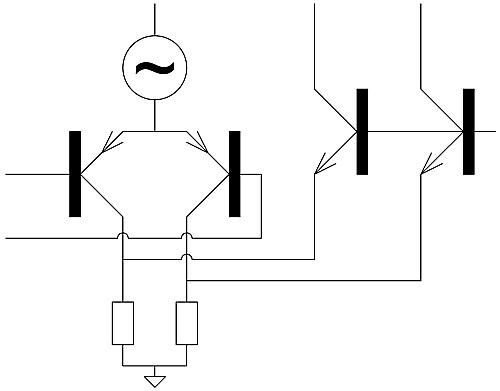
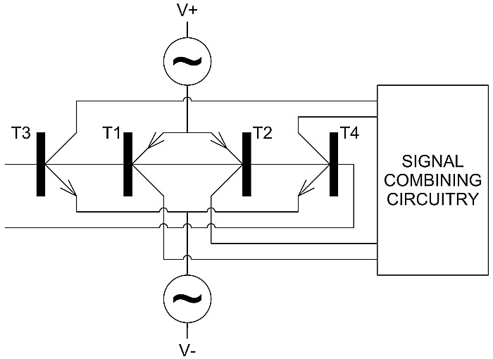
It is not possible to design a long tailed pair with CMR extending from its positive to its negative rail. (It is, of course, possible to put an inverter inside an op amp to generate extra supplies so that the input CMR includes both the external supplies but this technique is potentially noisy and the input stage is then not really a true rail rail device. When this article was written such amplifiers were not economically practicable - now, 20 years later, there are a few rail-rail amplifiers of this type.) Most op amps with rail rail inputs actually have two input stages, as shown in Fig. 5.
Fig 5. A "Rail-Rail" Input Stage.
What we have is a PNP long tailed pair, T1 and T2, which work with inputs at the negative supply and an NPN long tailed pair, T3 and T4, which works when the CMR approaches the positive supply. In between they both contribute, and their outputs are combined in the second stage of the op amp.
It is evident that when the CMV is high T1 and T2 will be turned off and only the Ib of T3 and T4 will flow, and when the CMV is low T3 and T4 will be off and T1 and T2 on. Thus not only will such a stage have relatively high bias current, for the same reasons as the single supply stage described above, but that current will change direction as the CMV changes.
We thus see that a rail rail input stage, though useful in many applications, is not ideal from the point of view of low Ib, stable Ib or complexity. However its Ib+ and Ib- do match quite well. Nevertheless it is wise not to use such a device unnecessarily as, apart from the rail rail performance, all the other parameters can be improved on in a more conventional device.
The final op amp we shall discuss is the transimpedance or current feedback type. This is quite different from a traditional (voltage feedback) type in having quite distinct characteristics on the inverting and non inverting inputs. The inverting input is a high impedance input similar to that of a voltage feedback op amp, but the inverting input is low impedance (~25Ω) which is held at the same potential as the non inverting input. The structure is used because of its excellent behaviour in wideband applications - which is outside the range of this article. It has low Vos and excellent voltage noise.
From the point of view of Ib, however, its behaviour is somewhat less convenient. All the types of amplifier we have discussed so far have some degree of correlation between Ib+ and Ib-. The transimpedance amplifier has none - the two bias currents are not matched, have different TCs, are bipolar (i.e. they may flow in either direction), and are relatively large. This would cause major difficulties in low frequency high precision applications, but is not actually a major problem in the HF applications for which transimpedance amplifiers were developed.
It is important to design the DC paths around a transimpedance amplifier with its bias currents in mind (you must read the data sheet!) but since most HF circuitry works at quite low impedance levels it is rarely difficult to achieve the DC performance required.
This article has described the possible variations and likely values of a single parameter of op amps, the bias current, Ib. When designing with op amps it is important to realise that, unlike the ideal in the text book, real op amps have bias currents which can vary widely:- from type to type, from device to device of the same type, with varying common mode voltage, and with temperature. If we assume that Ib is always zero we are likely to be in severe trouble, but if we take pains to understand the nature of Ib and the actual values and behaviour to be expected from the devices we are using it is rarely hard to incorporate its bias current into our design equations and achieve a successful and practical design.
Newbury - England 1995-08-05
Revised 2015-10-10
[Note that although this has been revised, many of the examples still date back 20 years to the original article.]